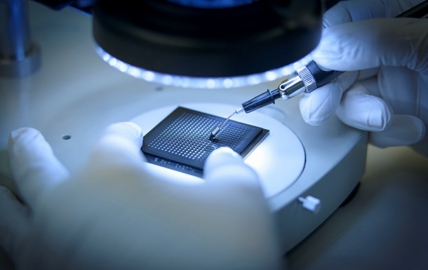
Photo: Getty Images (illustrative photo)
Scientists at Fudan University in Shanghai have created a hybrid chip that combines two-dimensional memory modules that are one atom thick with a traditional silicon architecture.
The basis of the new technology was the Atom2Chip system, which allows integrating a monolayer of molybdenum disulfide directly onto the surface of a CMOS chip. The thickness of this material is only one atomic layer. To protect it from damage, the team developed a special protection system and a cross-platform architecture that provides a connection between the two-dimensional circuits and the silicon substrate.
The prototype is a 1 kilobyte NOR flash memory chip operating at 5 megahertz. It is capable of reading, writing, and erasing data on external commands, with a programming or erasing time of only 20 nanoseconds.
Integrating 2D materials with silicon structures helps overcome the physical limitations of further miniaturization of semiconductors. Traditional silicon technology has already reached the limit of reducing transistor sizes, while 2D materials open up prospects for creating ultra-thin and powerful electronic components.
According to the researchers, this technology could become the basis for a new generation of processors and chips, combining extreme compactness with high performance.